Choosing Low‑Loss Materials for High‑Frequency Circuits
- As wireless systems push into mmWave and beyond, selecting low‑loss materials is becoming central to preserving signal integrity and reducing transmission losses.
- Engineers must weigh dielectric performance against manufacturability, thermal behavior and cost when choosing substrates for 5G/6G, radar and high‑speed digital links.
- Market forecasts predict a substantial rise in demand for these materials over the next decade, prompting suppliers and OEMs to reassess material choices and supply strategies.
Types of low‑loss materials
Manufacturers broadly classify low‑loss materials into organic, inorganic and composite families, each offering distinct trade‑offs between electrical performance and production practicality. Organic laminates such as PTFE, LCP and specialized epoxies are popular because they can deliver low dissipation factors while remaining compatible with common PCB processes. Inorganic options like LTCC and certain glasses tend to show very stable dielectric behavior and low moisture uptake, but they often require different manufacturing flows and can be more costly to integrate. Composite systems that blend polymers with ceramic or glass fillers aim to combine the electrical advantages of organics with the mechanical and thermal stability of inorganics.
Market dynamics are shifting as telecom and automotive applications demand both higher frequencies and higher volumes. Suppliers such as Celanese, Kyocera and Isola are among those developing materials tuned for mmWave and high‑speed digital use cases. Industry reports indicate that demand for low‑loss materials could grow several‑fold by 2036, driven by 5G densification, automotive radar adoption and eventual 6G rollouts. Designers therefore face a widening set of options but also greater pressure to match material choice to application constraints.
Key material properties to consider
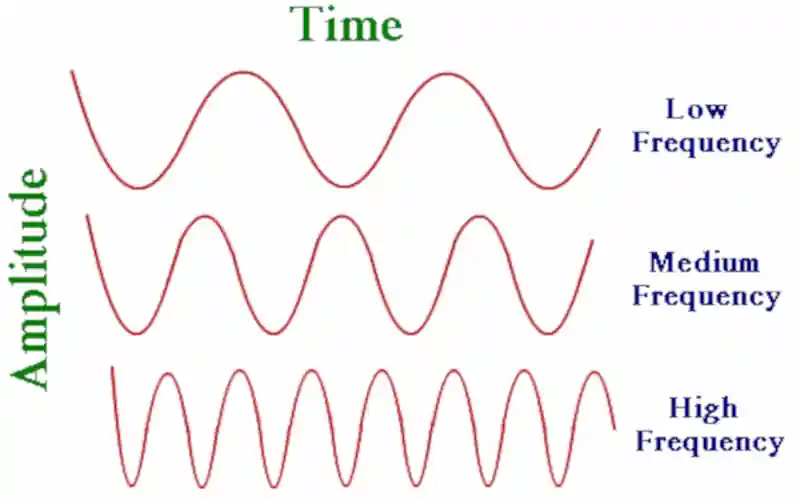
Dielectric constant (Dk) and loss tangent (Df) remain the primary electrical metrics when evaluating substrates for RF and high‑speed digital circuits. Stable Dk across the operational frequency band is essential because variations can change characteristic impedance and introduce reflections or timing errors in high‑speed traces. Thermal and mechanical properties such as coefficient of thermal expansion (CTE) and thermal conductivity are equally important, since mismatches with copper or component packages can cause warpage, delamination or solder joint failures under thermal cycling. Moisture absorption and copper foil roughness also affect long‑term signal integrity, with higher moisture uptake increasing insertion loss and rougher foils amplifying skin‑effect losses at mmWave frequencies.
Material selection therefore requires balancing electrical performance with manufacturability and reliability. Organic laminates offer tunable Dk/Df through resin chemistry and filler content, but their properties can vary more with temperature and humidity than ceramics. In contrast, LTCC and certain glass substrates provide low and stable Df over wide frequency ranges, yet they may impose limits on component mounting and routing density. Composite approaches can mitigate some of these trade‑offs, but they introduce complexity in process control and cost modeling.
Design and process implications
PCB stackup, trace geometry and copper treatment interact closely with substrate choice to determine final RF performance. Engineers must account for skin depth effects at mmWave frequencies, which make conductor surface roughness and plating quality significant contributors to loss. Signal routing strategies such as controlled impedance lines, differential pairs and via design must be validated against the chosen material’s Dk profile to avoid timing skew and insertion loss. Thermal management strategies, including heat spreading and material thermal conductivity, become critical in high‑power transceivers and data‑center interconnects.
Manufacturers also need to consider supply chain and cost implications when specifying materials at scale. Some high‑performance laminates remain niche and command premium pricing, which can be difficult to justify for cost‑sensitive consumer devices. Volume production for automotive radar and telecom infrastructure, however, can absorb higher material costs if reliability and performance gains translate into system‑level benefits. Collaboration between OEMs, board houses and material suppliers is therefore essential to align specifications, qualification cycles and cost targets.
Market outlook to 2036
The next decade will push materials into new frequency regimes as 77–79 GHz automotive radar becomes standard and 6G research moves toward sub‑THz bands. Achieving low dielectric loss at those frequencies is only part of the challenge; materials must also be processable in high volumes, stable across environments and cost‑effective for broad deployment. IDTechEx’s recent forecast projects a multi‑fold increase in demand for low‑loss materials, reflecting growth across telecom, automotive and data‑center markets. Suppliers that can demonstrate consistent performance, scalable manufacturing and regional supply resilience are likely to gain traction.
Industry roadmaps suggest that innovation will come from both chemistry and process engineering. Improvements in resin systems, filler technologies and copper foil treatments are expected to reduce losses while preserving manufacturability. At the same time, alternative substrate platforms such as advanced ceramics and glass composites may find niche roles where environmental stability is paramount. Buyers and designers should therefore maintain flexible sourcing strategies and invest in early qualification to avoid late‑stage redesigns.
Practical benchmarking matters: independent reports now compare more than 150 commercially available low‑loss materials across Dk, Df, moisture absorption, CTE and thermal conductivity, providing engineers with empirical data for trade‑offs. The industry is also seeing renewed interest in copper foil engineering—ultra‑smooth foils and specialized plating can cut conductor loss at mmWave frequencies by reducing skin‑effect penalties. Finally, regulatory and automotive qualification cycles are lengthening lead times for new materials, so early engagement between system architects and material suppliers is increasingly important to meet product launch schedules.